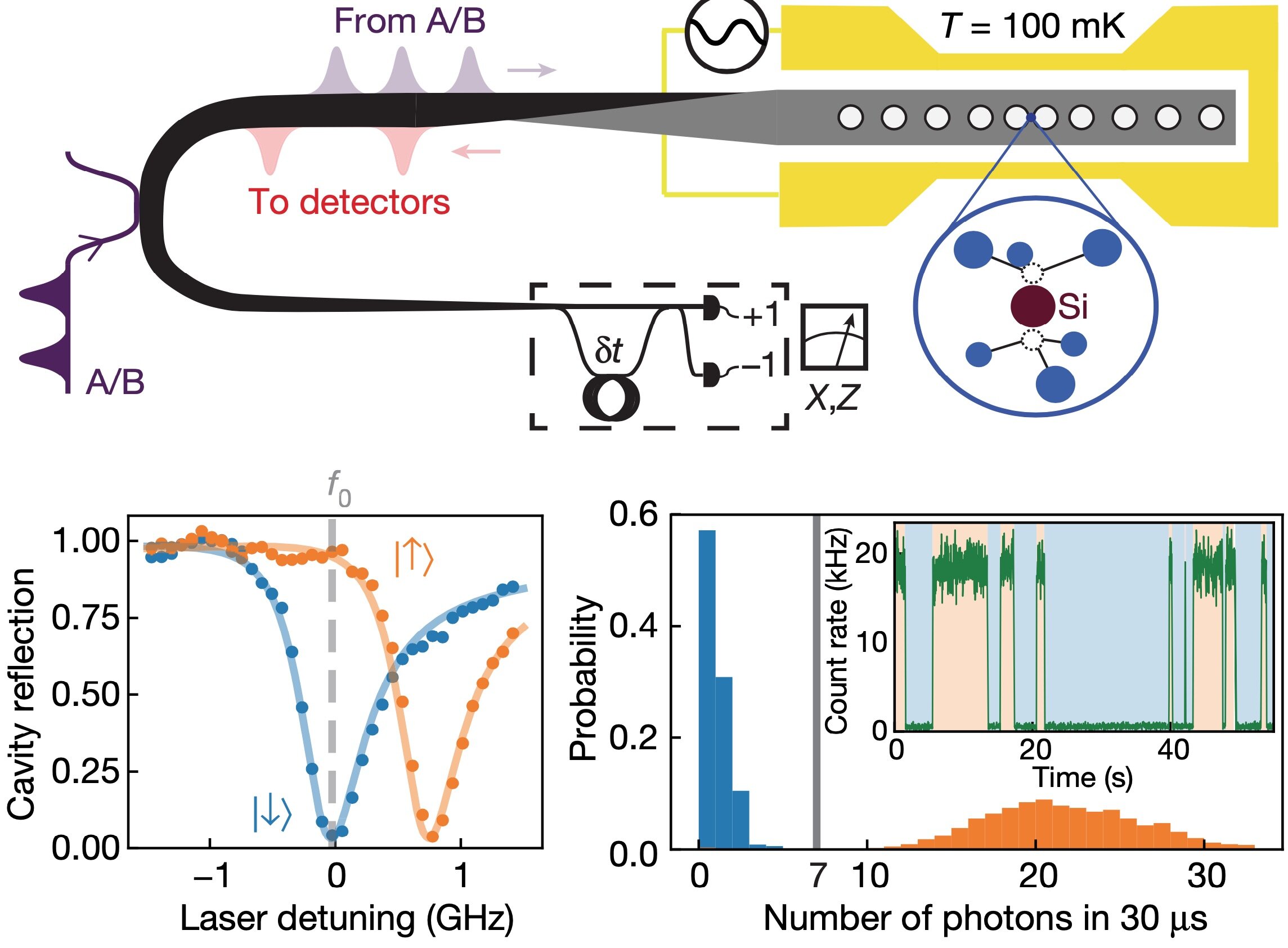
Quantum Optoelectronics
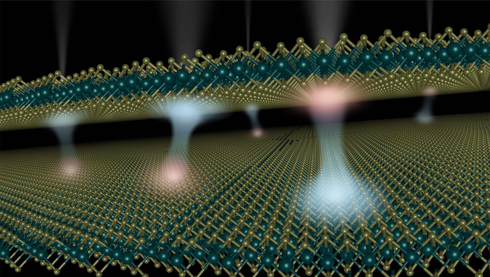
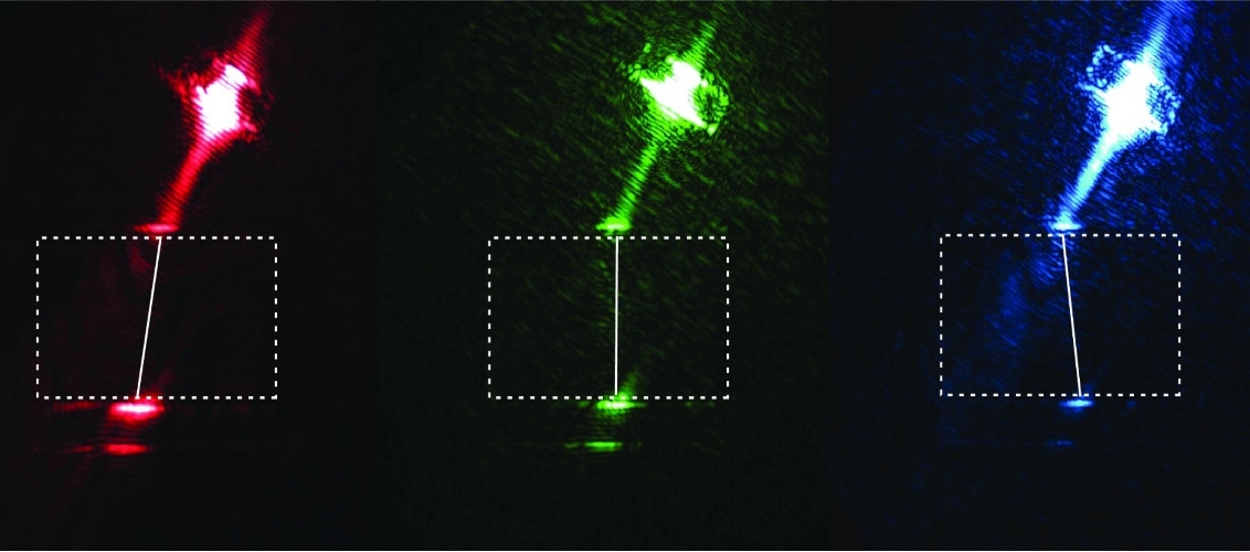
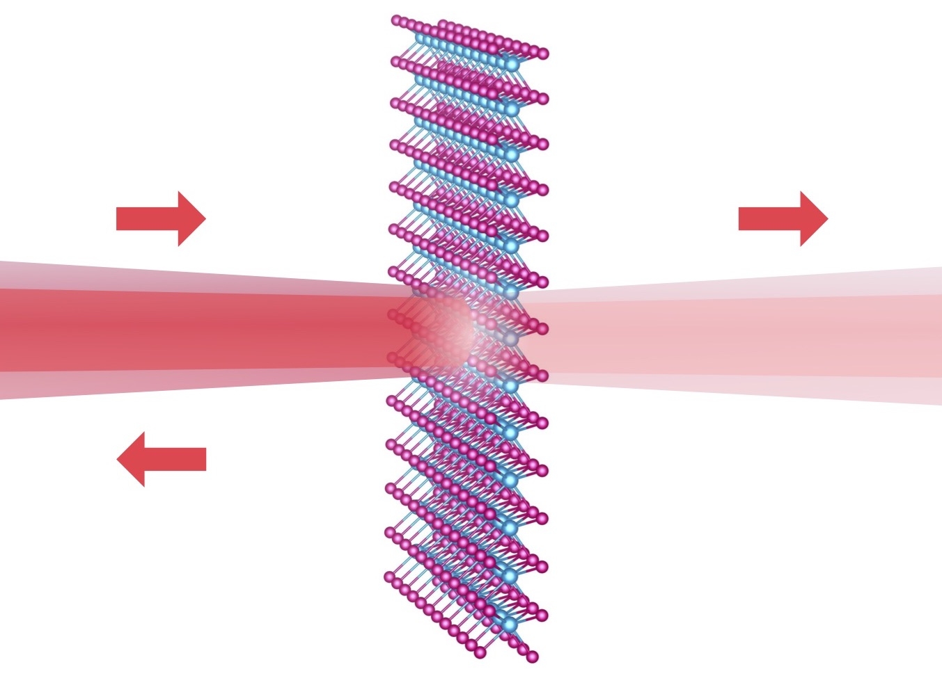
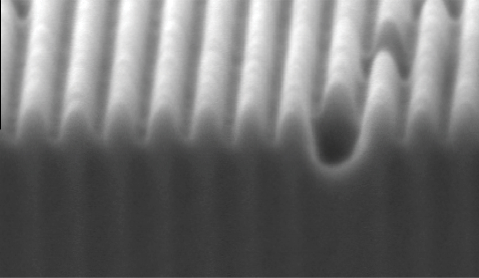
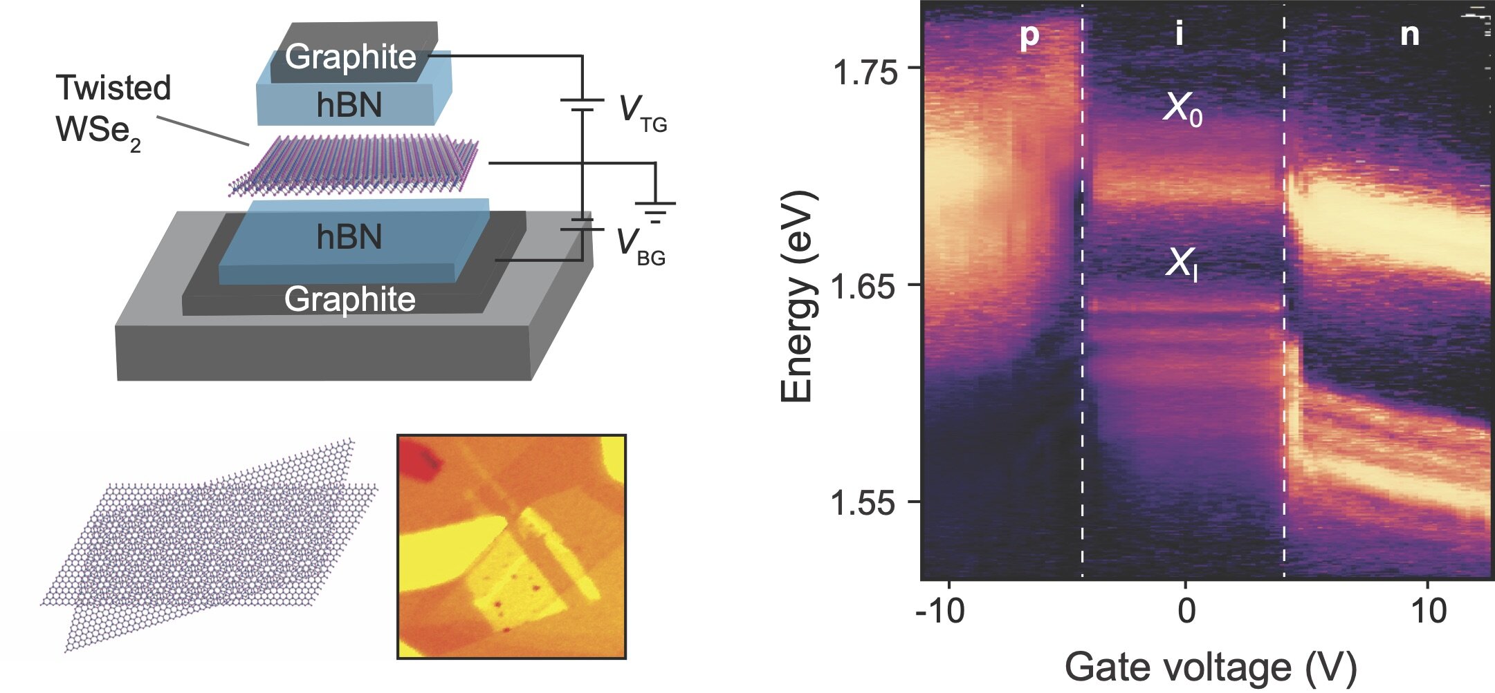
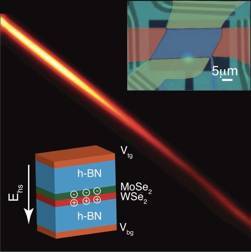
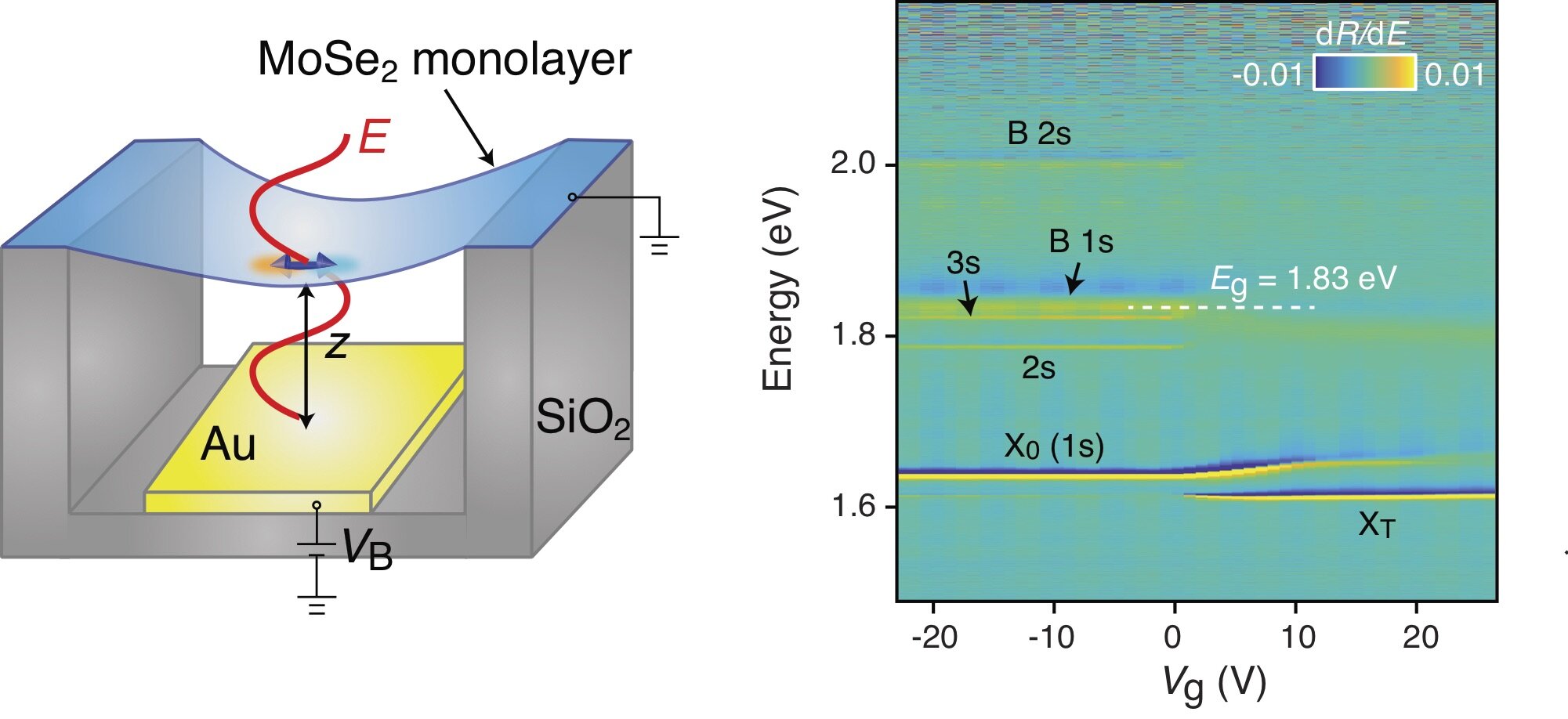
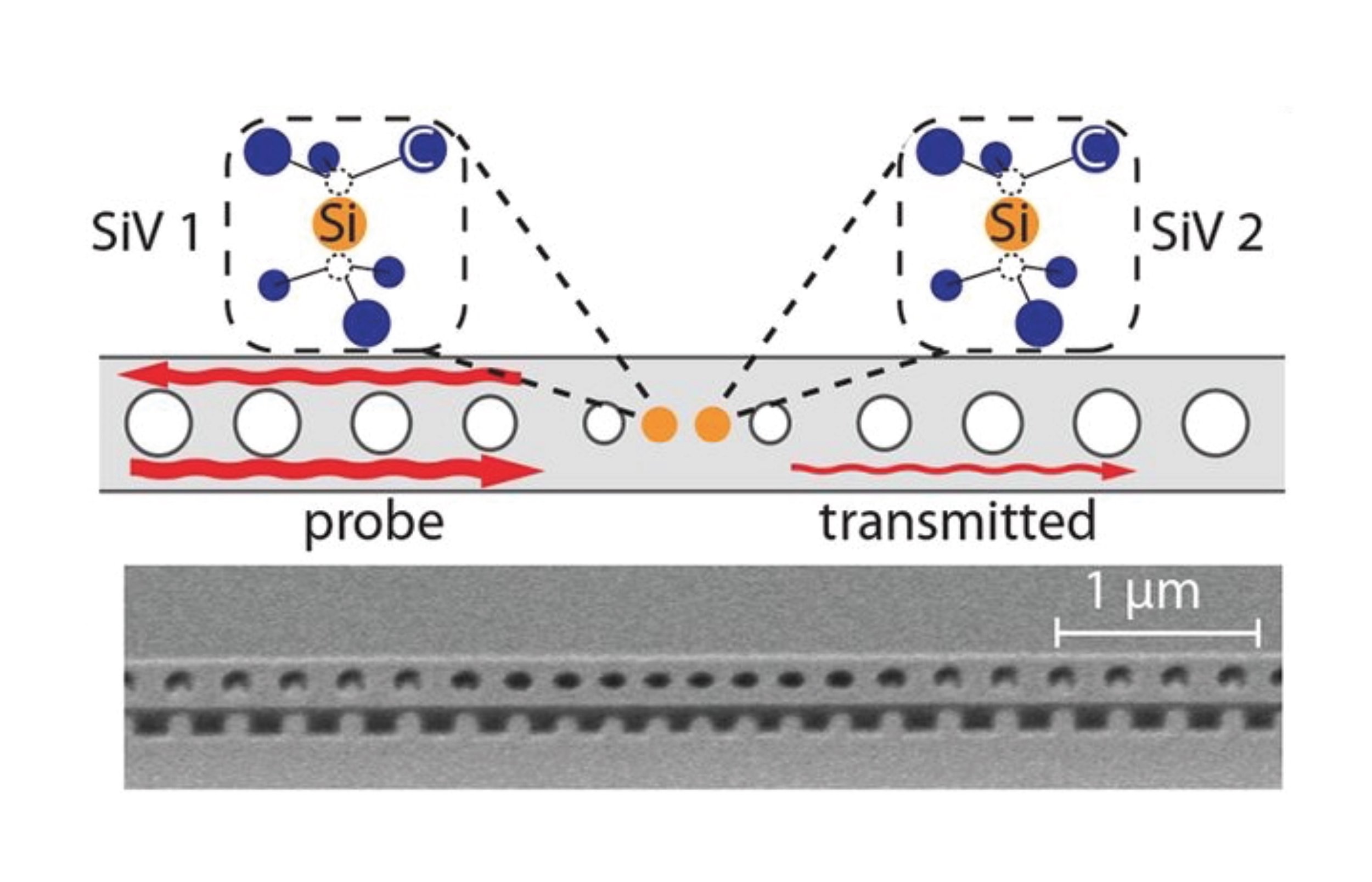
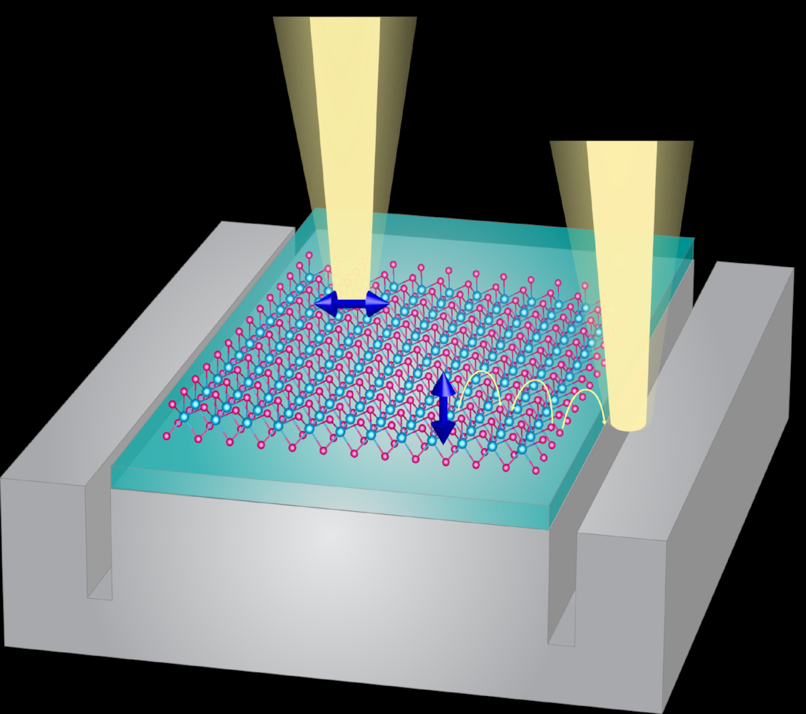
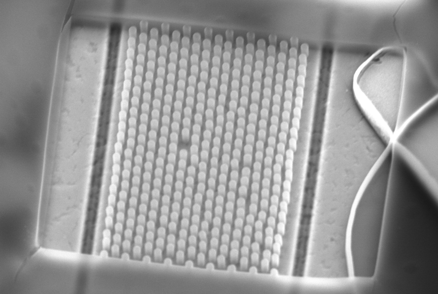
Nanoscale materials represent a natural size limit of the miniaturization trend of current technology, and they exhibit physical and chemical properties significantly different from their bulk counterparts. The Park group is exploring atom-sized defects in solids, atomically thin materials, and photonic and plasmonic nanostructures to realize solid-state optoelectronic and plasmonic devices that work all the way down to the single quantum level. Some examples of these devices include single-photon transistors, electrically driven quantum plasmonic switches, and topological quantum photonic circuits. These devices, whose operation is critically dependent upon quantum mechanical principles, may enable all-optical computing and solid-state quantum information processing.
Quantum melting of bilayer Wigner crystals studied in the absence of magnetic fields or moiré potentials in an atomically thin transition metal dichalcogenide heterostructure
Reconstructed domains of twisted MoSe2/MoSe2 bilayers exhibit interlayer excitons with opposite electric dipole moments
Quantum optoelectronic circuits on atomically thin van der Waals heterostructures
Refraction of surface plasmon polaritons at the flat silver/metasurface interface.
Excellent coherence properties of excitons in monolayer semiconductors enable efficient resonance reflection.
A cross-sectional scanning electron microscope image of a metasurface.
Schematic of a memory-assisted spin-photon gate consisting of a diamond nanophotonic resonator with a SiV quantum memory
Electrically tunable valley dynamics in twisted WSe2/WSe2 bilayer devices
Optical and electrical generation of long-lived neutral and charged interlayer excitons in atomically thin semiconductor heterostructures
Dynamic manipulation of excitons in a MoSe2 monolayer by suspending it over a metallic mirror
Photon-mediated interactions between silicon-vacancy color centers coupled to a diamond nanophotonic cavity
Probing dark excitons in atomically thin semiconductors via near-field coupling to surface plasmon polaritons.
Scanning electron microscope image of a plasmonic crystal cavity.